NANOXEROGRAPHY-MAKING OF LIGHT-EMITTING 2D METASURFACES
NANOSCIENCE

Lab: LPCNO
Duration: NanoX master Internship (8 months part-time in-lab immersion)
Latest starting date: 15/10/2025
Localisation: LPCNO
Institut National des Sciences Appliquées
135 avenue de Rangueil, 31077 TOULOUSE CEDEX 4 – FRANC
Supervisors:
Laurence RESSIER laurence.ressier@insa-toulouse.fr
Aurelien CUCHE aurelien.cuche@cemes.fr
This research master's degree project could be followed by a PhD
Work package:
Introduction and context - In order to face the future challenges in communication and data processing,
integrated optics and in particular nanophotonics offering deep integration at the nanoscale [1], is an
appealing approach that might lead to disruptive technologies. Thus, the development of advanced
integrated light-emitting optical components is mandatory to support this trend. An approach based on
individual optically resonant nanostructures (‘nanoantennas’) has demonstrated the capability to control
the emission of quantum emitters (QE) accurately positioned in their optical near field [2]. It has been
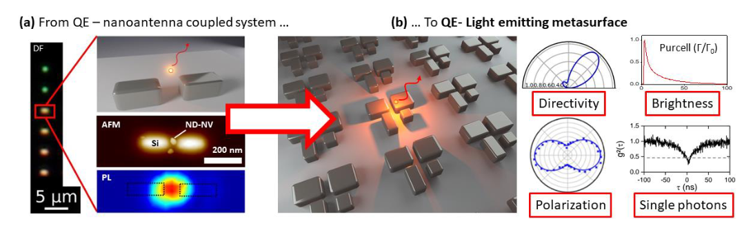
extensively explored, notably by the partners (Fig 1(a)), unveiling the complex mechanisms of this
coupling. Yet performances of QE-nanoantennas have reached a plateau as the number of degrees of
freedom is limited. Our project provides therefore an original path for a breakthrough with the design, the
fabrication and the characterization of complex plasmonic, dielectric or hybrid metal-dielectric light-
emitting 2D metasurfaces for the control of accurately positioned QE. Topic - The Q-META project aims
to control and enhance the emission properties of quantum emitters (QE) with 2D optical metasurfaces,
well beyond performances offered by the single nanoantennas at the state-of-the-art (Fig 1(a)). To do so,
the nanosources of non-classical light will be accurately positioned in the near field of 2D plasmonic and
dielectric arrays. The latter will be specifically designed to control the directivity, brightness, chirality,
polarization of the QE emission via coupling to localized and collective resonances, in the visible/near
infrared. In this project, the quantum emitters will be colored centers in colloidal nanodiamonds, with
typical diameters of few tens of nanometers [4]. NV centers will be preferentially used, but others colored
centers available at CEMES will be considered too (collaboration with an academic partner). These
different emitters will be systematically characterized by optical methods on operational time-resolved
confocal microscopes at CEMES. Wavelength-dependent lifetime measurements and intensity correlation
will be used to analyze their temporal dynamics. The dielectric and plasmonic metasurfaces will be
fabricated by ebeam lithography either on silicon on insulator (SOI) substrates for dielectric structures,
thanks to an active collaboration with the LAAS laboratory at Toulouse, or on glass/ITO substrates at
CEMES for plasmonic structures. Moreover, the geometry of these 2D metasurfaces will be optimized by
the mean of electrodynamic simulations available at CEMES (Green dyadic method (GDM) coupled to an
evolutionist optimization (eo) multi-objectives algorithm) [5]. The spatial and quantitative positioning of
the fluorescent emitters in the 2D periodical structure of the metasurfaces will be performed by a directed
assembly technique called AFM nanoxerography [6,7]. This technique has been developed in the Nanotech
team of LPCNO. It relies on the local injection of electrostatically charged dots by the mean of a polarized
AFM tip positioned above the areas of interest. These charged dots will act as selective electrostatic traps
for the emitters. The two labs (CEMES and LPCNO) involved in that project recently demonstrated the deterministic and reproducible positioning of nanodiamonds on a flat SiO2/Si film (Fig 2) [8] and on singlesilicon nanoantennas (Fig 1(a)) [3]. Once the emitter-metasurface hybrid systems are done, the wavelength-
and (dipole) orientation-dependent modification of the photodynamics of the emitters will be measured by
2D mapping of the time-resolved photoluminescence. The directivity and polarization control will be
assessed by polarization-resolved back-focal plane imaging. These optical characterizations will be
performed at CEMES on state-of-art time-resolved confocal microscopes. The experimental results will be
systematically supported by GDM-based simulations.

References:
References: [1] AF. Koenderink et al. Science 348, 516 (2015) [2] AF. Koenderink et al. ACS Photon 4,
710 (2017) [3] M. Humbert et al. Nanoscale, 15, 599 (2023) [4] M. Humbert et al. Phys. Rev. Applied 17,
014008 (2022) [5] P. R. Wiecha et al. Nature Nano 12, 163 (2017) [6] P. Moutet et al. Nanoscale 7, 2009-
2022 (2015) [7] N. M. Sangeetha et al. Nanoscale 5, 9587 (2013) [8] M. Humbert et al. Nanotech. 33,
215301 (2022)
Areas of expertise:
Quantum technologies, single photon sources, colored centers, nanodiamond, high-
index dielectrics, plasmonics, metasurfaces, time-resolved optical microscopy,
photon correlation, directed assembly, nanoxerography, Atomic Force
Microscopy (AFM), numerical simulation of optical properties.
Required skills for the internship:
The candidate will be involved in the experimental aspects of (i) electrical and
topographical modes of AFM, (ii) the process of directed assembly of the quantum
emitters by nanoxerography, (iii) the optical characterization at the single photon
scale (quantum regime), and to the theoretical aspects of (iv) the methods of
electrodynamics simulation and of the design of the structures by eo algorithm.
Autonomy, dynamism, scientific curiosity and rigor are the key words to carry out
this project.
