
MICRO-NANO-FABRICATION FOR MAGNETIC METAMATERIALS NANOSTRUCTURES
NANOSCIENCE
Lab: CEMES
Duration: NanoX master Internship (8 months part-time in-lab immersion)
Latest starting date: 12/10/2026
Localisation: CEMES, 29 Rue Jeanne Marvig, 31055 Toulouse
Supervisors:
Christophe GATEL christophe.gatel@cemes.fr
Justine HARMEL justine.harmel@cemes.fr
Work package:
With the rapid miniaturization of devices, such as transistors—a building block of the semiconductor industry—now smaller than 5 nm, this reduction in scale opens new perspectives for exploring remarkable properties at this scale.
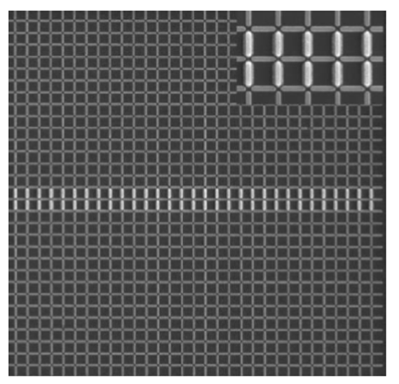
The ANR MetaCharge project aims to exploit nanofabricated magnetic metamaterials as experimental platforms to emulate and visualize, in real time and at the nanoscale, fundamental charge transport phenomena. Using two-dimensional arrays of nanomagnets, the project seeks to establish a link between frustrated magnetism and the physics of electron transport. The success of this project depends crucially on the controlled fabrication of thermally active metamaterials compatible with advanced operando imaging techniques, particularly transmission electron microscopy.
In this context, the cleanroom intern recruited at CEMES will play a central role in the development and optimization of the samples. The intern will be responsible for the development and implementation of nanofabrication processes (multi-step electron beam lithography, thin film deposition, lift-off, etching…) for the fabrication of nanomagnet arrays on Si₃N₄ membranes for TEM experiments. The intern will also contribute to adapting the processes to the specific constraints of dynamic experiments (thermal stability, reproducibility, structural quality), do the link with experimental observations, and will participate in the development of cleanroom protocols, thus ensuring the experimental feasibility and scientific quality of the project.
The micro-nanofabrication of nanomagnet arrays will utilize cleanroom techniques such as laser lithography, electron beam lithography, thin-film deposition, and etching or lift-off for the fabrication of the complete device. Among the processes studied, the use of Si₃N₄-based membranes will be essential. These silicon nitride thin membranes will enable high-temperature operation and real-time in-situ transmission electron microscopy (TEM) observations.
References:
References: "Through-membrane electron-beam lithography for ultrathin membrane applications." Neklyudova, M., et al. Applied Physics Letters 111.6 (2017).; “Concept of imaging spin waves in pseudo-static mode by electron holography” Marine Resano, Christophe Gatel, Abraao Cefas Torres-Dias, Benjamin Lassagne, Nicolas Biziere; Appl. Phys. Lett. 24 November 2025; 127 (21): 212404
Areas of expertise:
Micro- and nanofabrication techniques; laser lithography; electron beam lithography; chemical etching; electrical measurements
Required skills for the internship:
ability to work in a cleanroom; adherence to safety regulations; autonomy; scientific curiosity and methodology.