
Photoluminescence imaging of quantum emitters coupled to dielectric nanoantenna
NANOSCIENCE
Lab: CEMES
Duration: NanoX master Internship (8 months part-time in-lab immersion)
Latest starting date: 03/10/2022
Localisation: CEMES
Supervisors:
Prof. Vincent Paillard vincent.paillard@cemes.fr
Dr Gonzague Agez gonzague.agez@cemes.fr
This research master's degree project could be followed by a PhD
Work package:
For several years, nanoscale optics was driven by plasmonics since noble metal nanoantennas support surface plasmon resonances that can be used to manipulate, concentrate or redirect visible light. These very appealing properties for potential applications in integrated optics, sensors, nonlinear optics, or field-enhanced spectroscopy are however limited by the large internal losses in the metal due to high optical absorption.
An alternative approach emerged with optically resonant high-index dielectric nanostructures (NS) [2]. Such NS, by manipulating Mie optical resonances via their size and shape and the constituent material, offer the same properties and applications as plasmonic NS, with the advantages of much weaker absorption losses at optical wavelengths, and the access to semiconductor processing technologies for nanofabrication. Therefore, silicon (Si) is an excellent candidate with a high refractive index, a low extinction coefficient in the visible to NIR spectrum, and a perfect control of nanostructure fabrication.
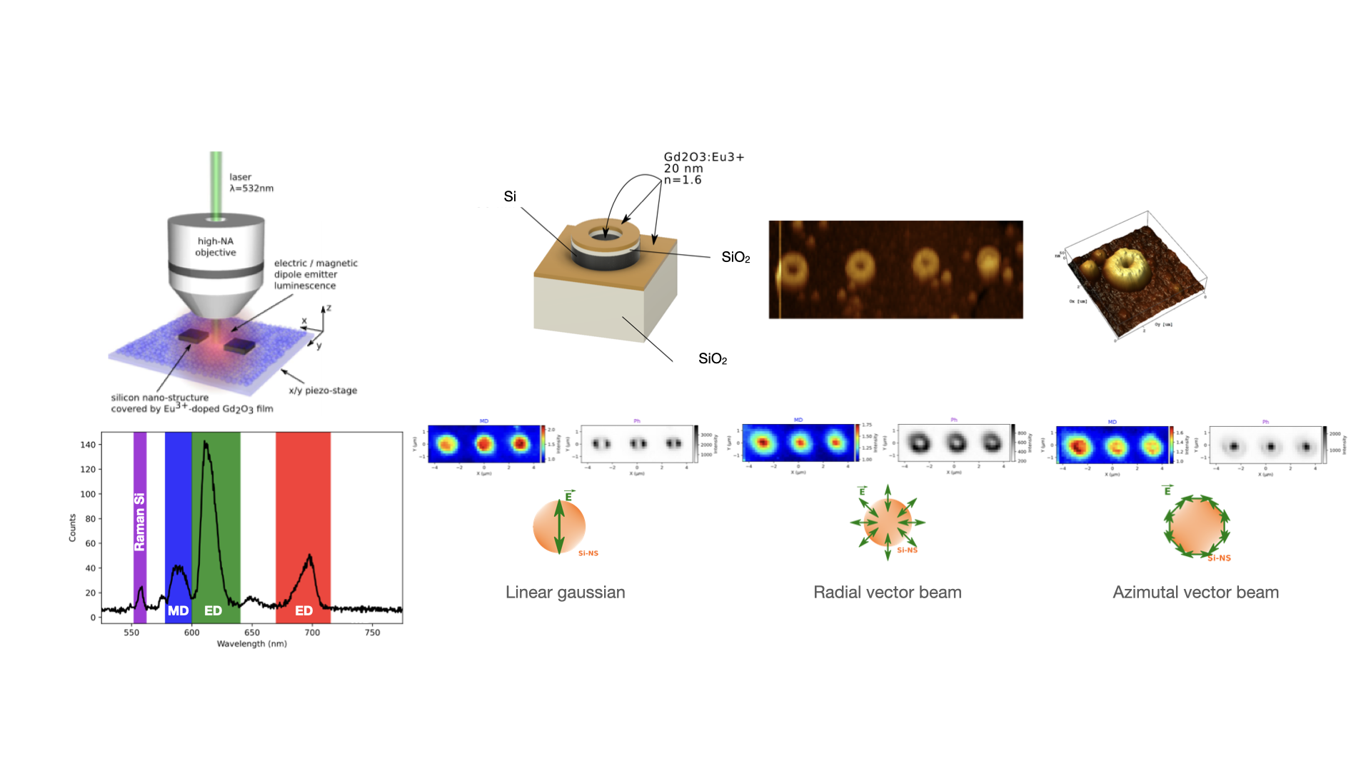
The master internship subject is focused on the coupling of Si nanostructures to quantum emitters, which is crucial for the development of photodetectors, solid-state lighting, and photon sources at the nanoscale. Recently, we have shown that the photoluminescence (PL) mapping of emitters positioned in the near field of Si-NS can be spatially engineered either via the photon local density of states (LDOS), or the beam shape and polarization of the laser (linear gaussian or azimutal or radial vortex beam).
New samples have been fabricated with optimized shapes and dimensions of Si nanoantennas covered with a thin Eu3+-doped film. The aim of the internship is to characterize the samples by PL mapping in different configurations and compare the experimental results to numerical simulations.
References:
General references on the topics:
- Antennas for light, L. Novotny, and N. van Hulst, Nat. Photon. 5, 83 (2011)
- Excitation of Magnetic Dipole Transitions at Optical Frequencies, M. Kasperczyk et al, Phys. Rev. Lett. 114, 163903 (2015)
- Optically resonant dielectric nanostructures, A. Kuznetsov et al, Science 354, 846 (2016)
- Dielectric nanoantennas to manipulate solid-state light emission, S. Bidault et al, J. Appl. Phys. 126, 094104 (2019)
Recent publications of the team on the topic
Evolutionary multi-objective optimization of color pixels based on dielectric nanoantenna, P. R. Wiecha, A. Arbouet, C. Girard, A. Lecestre, G. Larrieu, V. Paillard, Nature Nano 12, 163 (2017)
- Enhancement of electric and magnetic dipole transition of rare-earth doped thin films tailored by high-index dielectric nanostructures, P. R. Wiecha et al, Applied Optics 7, 1682 (2019)
Unveiling the optical emission channels of monolayer semiconductors coupled to silicon nanoantennas, J.-M. Poumirol, I. Paradisanos, S. Shree, G. Agez ... V. Paillard, B. Urbaszek.
ACS Photonics 7, 3106 (2020)
- Engineered near- and far-field optical response of dielectric nanospheroids using focused cylindrical vector beams, M. Montagnac, G. Agez, A. Patoux, A. Arbouet, V. Paillard, J. Appl. Phys. 131, 133101 (2022)
Areas of expertise:
Nano-optics, silicon antennas, Mie resonance, quantum emitters, light source at the nanoscale, optical spectroscopy, numerical simulations
Required skills for the internship:
Good education level in general physics (optics, electromagnetism, solid state physics, quantum physics), numerical skills (python), strong interest for both optical experiments and numerical simulations