
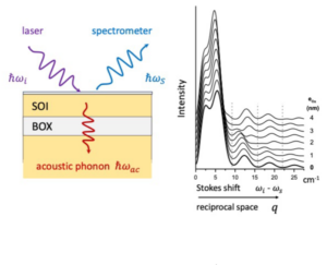
 left : schematic plot of inelastic light scattering by acoustic phonons in a Silicon On Insulator (SOI) on top of a Burried Oxide layer.
right : SOI acoustic phonon Raman spectra as a function of surface oxide layer.
The aim of the ADN project is to develop a new tool based on acoustics for probing doping profiles at the nanoscale in semiconductor heterostructures.
Owing to the dependence of sound velocities on doping level, we shall use high frequency acoustic phonons as internal probes in inelastic light scattering experiments. The ADN project aims to provide a proof of concept, to demonstrate the relevancy of our innovating approach. Our strategy is as follows: (i) provide experimental evidence of sensitivity by considering a large set of samples with selected and controlled doping and layer characteristics. (ii) achieve quantitative analysis by systematically comparing experimental and simulated spectra.
Inelastic light scatetring experiments will be performed using a Raman spectrometer.
(i) and (ii) will be implemented jointly with the support of complementary techniques, in particular micro-FTIR (Fourier-transform infrared spectroscopy), HRTEM (high resolution transmission electron microscopy) and STEM-EDX (scanning energy-dispersive X-ray spectroscopy). In order to carry out the ADN project we selected a model system based on doped Silicon On Insulator (SOI) layers with state of the art thickness control in the nanometer range.
Our approach has high potential, it is non-destructive and may apply to both n and p-type doping and to a wide range of materials.
CEMES (Centre d’Elaboration de Matériaux et d’Etudes Structurales)
NeO Team (Nano-Optics and Nanomaterials for Optics)
Jesse GROENEN – Jesse.Groenen@cemes.fr