
Research project selected under the 2019 call for proposals
Principal Investigator : Bernhard Urbaszek
Involved Teams :
- LPCNO / Quantum Optoelectronics Group
- CEMES / Nano-Optics and Nano-materials for optics – NeO
- LAAS / Materials and Processing for Nano-electronics – MPN
Type of project : Collaborative Project
Date (start/end) : 2019 – 2022
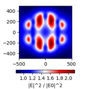
Two-dimensional transition-metal dichalcogenides (TMDs) such as MoS2 and WSe2 atomic monolayers (MLs) show great promise as versatile atomic-scale light sources for optoelectronics applications and optical spin-valley manipulation due to their strong and tunable light-matter interaction and compatibility with silicon (Si) photonics platforms. However, so far the emission efficiency of TMD MLs is limited and new approaches to simultaneously enhance light absorption, emission and control its directionality are required. In this project the 3 groups from CEMES, LAAS and LPCNO will couple TMD MLs directly to Si nanostructures with engineered optical near-field and far-field response. The consortium covers the complementary techniques required to (i) design nano-resonators with Mie resonances adapted to optical transitions in TMD MLs (ii) fabricate nano-resonator arrays on-chip compatible with Si-industry standards (iii) transfer highest quality, encapsulated TMD material on the resonators and (vi) use advanced optical techniques to analyze tailored emission intensity and directionality from the hybrid devices.