
Research project selected under the 2020 call for proposals
Principal Investigator : Laurent LOMBEZ 
Involved Teams :
- LPCNO / Quantum optoelectronics
Type of project : Disruptive Project
Date (start/end) : 2020 – 2023
Following the example of the graphene craze, the scientific community is interested in the properties of new 2D materials, associated in Wan der Waals hetrostructures, that have extraordinary optical and electrical properties. As the fundamental
properties of such materials is becoming more and more understood, it is important to measure charge and spin(valley) transport properties in order to develop optoelectronic and/or spin(valley)tronic devices.
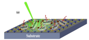
For optoelectronic application with 2D semiconductor materials, most of the research is focused on transition metal dichalcogenides (MoS2, MoSe2, WSe2, WS2…). Their optical properties are particularly remarkable (ex: very high absorption up to 20% per monolayer) and lead to the design of new ultra-thin optoelectronic devices. Also, good electrical conductivity is expected and recent progress has been made in particular thanks to the control of the dielectric environment via encapsulation with hexagonal boron nitride (h-BN) layers. Moreover, for the design of ultra-thin devices it is important to focus on excitons: strongly bound electron-hole pairs with binding energy of a few hundreds of meV, much larger than in conventional semiconductors. Therefore, the analysis of such a material will mainly measure the excitonic transport, which is thought to be at the basis of a new electronics. However, there are many challenges to understand the creation, transport and dissociations of the different excitonic particles. It is therefore fundamental to understand this complex transport and then try to control it; this is the main purpose of the project.
Yet it is important to measure carrier/excitonic transport and spin/valley properties in order to develop an optoelectronic and/or spintronic device. We should demonstrate the control of the transport properties via external factors such as strain, dielectric environment, electrical/chemical doping, temperature and obviously electric and magnetic field.
To face these challenges, optical measurement methods are ideal because they can be quantitative and measure electronic properties without electrical contacts (early stages of design), so before the creation of a final device.